Focused MeV Proton Beams: Applications in Nano-Lithography and Nanoscale-Imaging
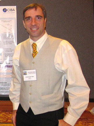
J.A. van Kan
Centre for Ion Beam Applications
Department of Physics
National University of Singapore
Présentation en anglais
En présentiel: Campus MIL, local B-2061
En ligne: vidéoconférence, Zoom #: 85795431636 (Zoom link)
Lorsque demandé, indiquer 'sept six un trois quatre huit' en chiffre.
Abstract: A second generation proton beam writing (PBW) line has been installed at the Centre for Ion Beam Applications at the National University of Singapore. PBW is a new direct write 3D nano lithographic technique which has been developed in Singapore. PBW employs a focused MeV proton beam which is scanned in a predetermined pattern over a resist, which is subsequently chemically developed. PBW exhibits low proximity effects coupled with the straight trajectory and even energy deposition along the path of the proton beam results in sidewall smoothness of a few nm root mean square. The high penetration depth of the proton beam enables the production of high aspect ratio, high density 3D micro and nano structures with smooth sidewalls, ideal for high quality mold production for nano-imprint-lithography (NIL) applications. The 2nd generation PBW system is now able to focus proton beams down to 9.3 x 32 nm2, revolutionizing applications of MeV proton beams [1], allowing high aspect ratio lithography down to 19 nm in HSQ.
Proton beam writing (PBW) is an ideal technique to fabricate lab-on-chip devices with features at the micron as well as at the nano scale. An easy method is introduced allowing fast replication of nanofluidic lab-on-chip devices using accurately fabricated molds featuring cross-sections down to 60 nm in polydimethylsiloxane (PDMS). High quality masters are obtained through PBW and UV lithography [2]. These masters can be used more than 200 times to replicate nanofluidic devices capable of handling single DNA molecules. This method reduces fabrication and packaging complexity, allowing end users to fabricate lab on a chip devices through simple PDMS casting. Using fluorescence microscopy the extensions of DNA molecules has been observed inside these PDMS nano-channels. Large scale DNA sequencing will be demonstrated [3].
We have recently also incorporated another new beam line: A high resolution single cell imaging facility. The new cell imaging facility has now been commissioned, and resolutions of 20-30 nm have been achieved for MeV proton and alpha particle beams [4]. The facility has been designed to utilize a variety of techniques, including Scanning Transmission Ion Microscopy (STIM) and Proton Induced Fluorescence (PIF) imaging. The interaction of MeV ions with biological material will be briefly discussed and some interesting results on structural and fluorescence imaging of whole cells using MeV ions will be presented.
References
[1] J.A. van Kan, P. Malar, and A. B. de Vera, Rev. Sci. Instrum., 83, (2012) 02B902-1 02B902-3.
[2] JA van Kan, C. Zhang, P. Malar and J.R.C. van der Maarel, Biomicrofluidics 6 (2012) 036502-1
[3] C Zhang, A Hernandez-Garcia, K Jiang, Z Gong, D Guttula, SY Ng, PP Malar, JA van Kan, Liang Dai, PS Doyle, R de Vries, and JRC van der Maarel, Nucleic Acids Research, 41 (2013) e189.
[4] F. Watt, X Chen, AB De Vera, CCN Udalagama, R Minqin, JA van Kan, AA Bettiol, Nuclear Instruments & Methods in Physics Research Section B 269 (2011) 2168–2174
Cette conférence est présentée par le RQMP.

