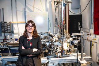
The electronic (and optoelectronic) devices that are ubiquitous in our modern world are driven by excitations: how electrons (and their empty counterpart holes) move through and interact with the environment they live in. But materials are never perfect, and defects in materials, disorder at interfaces, and even the structure of devices themselves change the world that electrons see. I will describe how the scanning tunnelling microscope – a remarkable tool that “sees” electrons in real space at atomic length scales – can help us understand the influence of disorder on the electronic states that underlie macroscopic devices.
With the STM as an exquisite tool for visualizing the local electronic environment, I will describe the picture we have built of how the electronic landscapes within organic semiconductors is influenced by structure. These materials, with low dielectric constants and minimal spin-orbit coupling present unique challenges for use in devices such as solar cells and light emitting diodes, despite the promise offered by chemical tuning and facile fabrication. Our work points to ways we may be able to work with instead of against the features of molecular systems to optimize materials for future devices.
- Cochrane, K.A., Schiffrin, A., Roussy, T.S., Capsoni, M. & Burke, S.A. Nat. Commun. 6, 8312 (2015).
- Cochrane, K.A. et al. J. Phys. Chem. C 122, 8437–8444 (2018).
- Mayder, D.M. et al. Chem. Mater. 34, 2624–2635 (2022).
Bio
Dr. Sarah Burke is an Associate Professor in the departments of Physics & Astronomy, and Chemistry, and a Principal Investigator in the Stewart Blusson Quantum Matter Institute at the University of British Columbia. Her research uses scanning probe microscopy techniques to investigate materials from the atomic scale up. Burke received her Bachelor’s Degree from Dalhousie University in 2002 (Honours in Physics) and her Master’s and Doctoral Degrees in Physics from McGill University in 2004 and 2009 respectively, where she focused on studying the growth and epitaxy of organic molecules on insulating surfaces using non-contact atomic force microscopy. She then held an NSERC Postdoctoral Fellowship at UC Berkeley with Michael Crommie where she investigated graphene nano-structures using low temperature scanning tunnelling microscopy and spectroscopy.
Since arriving at the University of British Columbia in 2010 she has built an interdisciplinary research group approaching materials questions from the atomic scale, applying these techniques to a wide range of materials from superconductors to molecular materials for future devices and controlling surface reactivity. She held the Canada Research Chair (Tier 2) in Nanoscience 2010-2020, received a Peter Wall Early Career Scholar Award for Interdisciplinary study 2011-2012, and the Killam Award for Excellence in Mentoring in 2022.

